COMMON-EMITTER COLPITTS OSCILLATOR

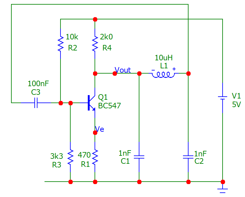
This is quite a popular Colpitts oscillator configuration. The schematic below shows a CE amplifier alongside a CLC filter. The magenta dotted lines show how the oscillator will connect and, the orange boxed parts are the components that define the operating frequency: -

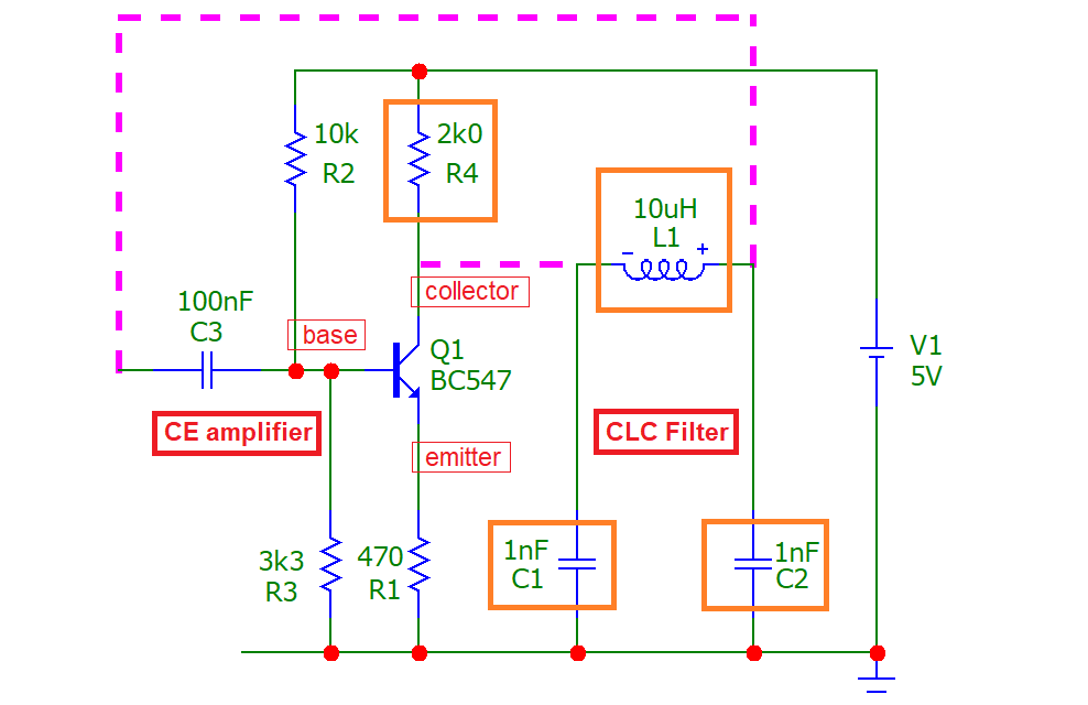
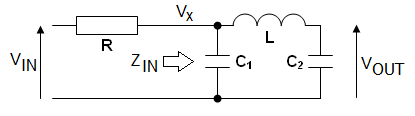
To analyse the circuit and derive the oscillation frequency formula, the collector node cannot be assumed to be unloaded. This mistake is made by many websites that attempt to describe functionality; important subtleties are glossed-over and, the formulas are presented matter-of-fact with no attempt to reveal the workings. Some websites misleadingly describe the operation by referring to a tank circuit (where C1 and C2 are in series) but, because C1 and C2 are grounded, they form a filter not only with inductor L1, but with resistor R4.


R4 makes this a 3rd order filter and only a 3rd order filter can produce sufficient phase shift for the circuit to oscillate. R4 is that important!


So, R4, C1, C2 and L1 form a 3rd order low-pass filter that produces 180° phase-shift whilst still providing sufficient signal gain to initiate and maintain oscillation. A 2nd order analysis is insufficient to deliver the theory. Bear that in mind. This is a proper analysis.


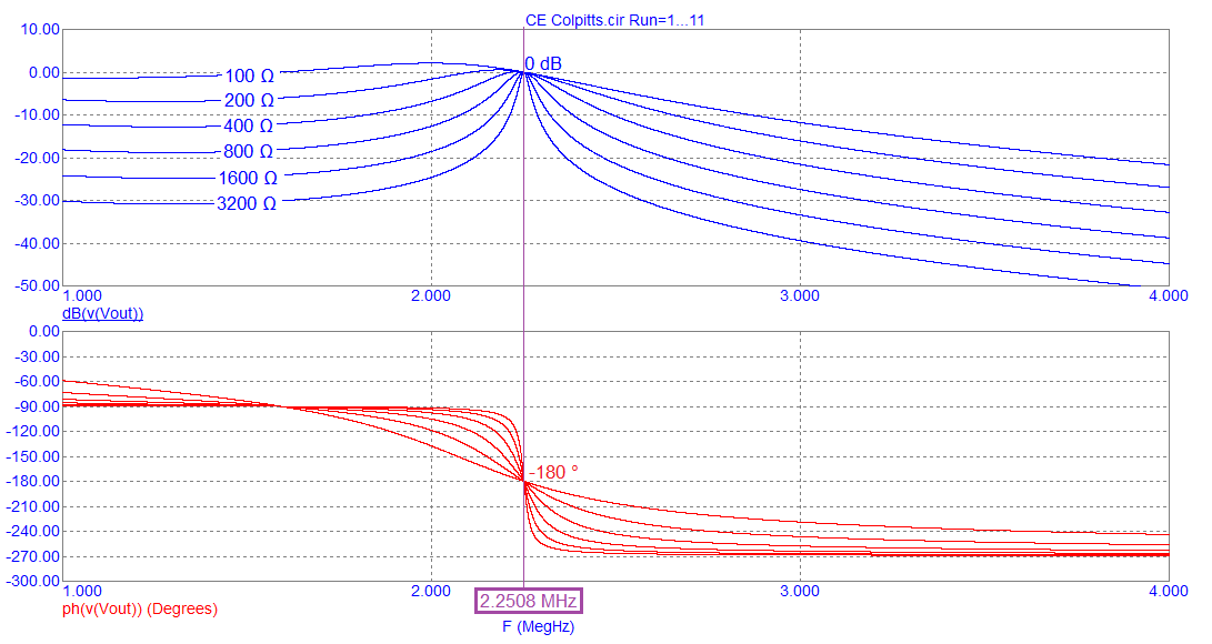
So, we "recognize" that Q1's collector is a current source in parallel with R4 and that this is equivalent to a voltage source in series with R4. Hence, R4 and C1 form a low-pass filter that introduces a lagging phase angle at the collector. Below is the bode plot when we apply a signal generator at the circuit input (C3) and C1 is connected to the collector (L and C2 are not connected yet): -

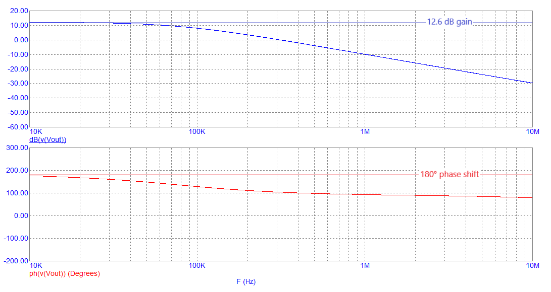
Normally, a CE amplifier delivers constant gain across a wide frequency range (with a phase angle of 180°) but, with C1 loading the collector, the phase shift is tending towards +90° at high frequencies. The gain is also reducing at high frequencies. The faint lines in the diagram above show the natural gain of the CE amplifier (12.6 dB). This gain is due to the ratio of R4 to R1 i.e. 2000 ÷ 470 = 4.255 = 12.6 dB.


Then, if L and C2 are added to R4 and C1 we get this bode plot after inductor L1: -

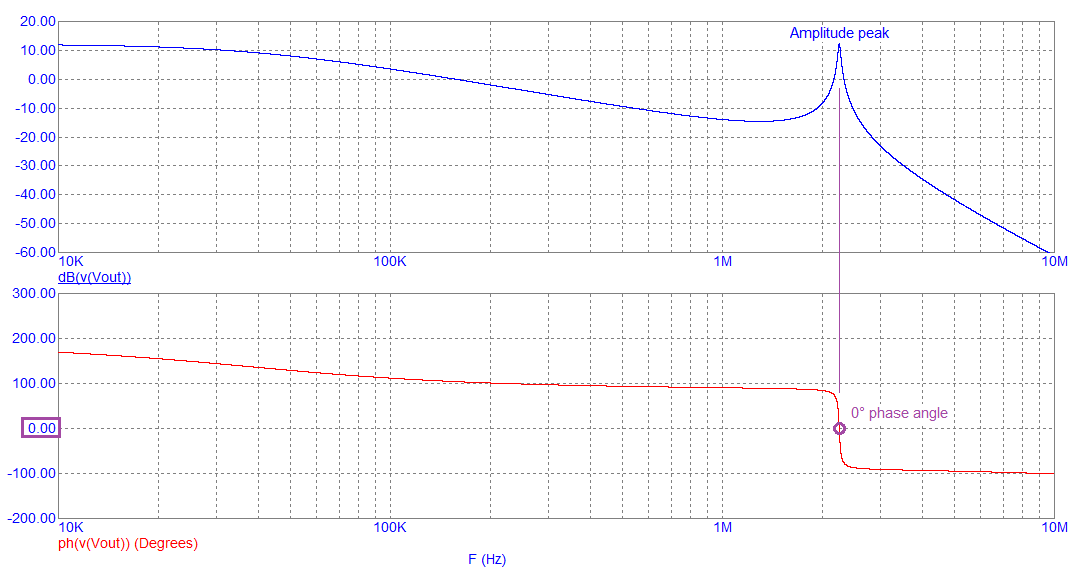
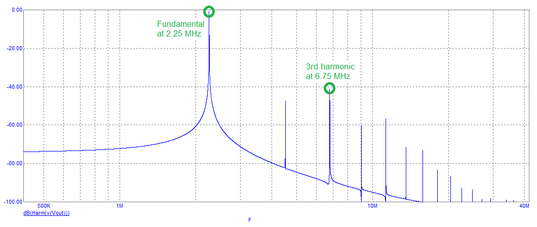
Note that the amplitude peak at about 2 MHz corresponds with a 0° phase angle. When the feedback loop is closed, this is where the circuit will oscillate. The 0° phase shift is a result of the collector resistor (R4) feeding C1, L and C2 i.e. this is a 3rd order filter. The gain peak at around 2 MHz is 12.6 dB because, at the oscillation frequency, when C1 equals C2, the 3rd order filter has unity gain. This is shown below: -


3rd order analysis of the operating frequency


Firstly, consider \(V_{OUT}\) in terms of \(V_X\): -


\(\dfrac{V_{OUT}}{V_{X}} = \dfrac{\frac{1}{sC_2}}{\frac{1}{sC_2} + sL} = \dfrac{1}{1+s^2LC_2}\)


Next, consider the impedance of \(Z_{IN}\): -


  \(Z_{IN} = \dfrac{\left[\frac{1}{sC_2}+sL\right]\cdot\frac{1}{sC_1}}{\frac{1}{sC_1}+\frac{1}{sC_2} +sL} = \dfrac{\left[1+s^2LC_2\right]\cdot\frac{1}{sC_1}}{1+\frac{C_2}{C_1} +s^2LC_2}\)


\(Z_{IN} = \dfrac{1+s^2LC_2}{s^3LC_1C_2+s(C_1+C_2)}\)


Then, consider \(V_X\) in terms of \(V_{IN}\) by using \(Z_{IN}\): -


\(\dfrac{V_X}{V_{IN}} = \dfrac{1 + s^2LC_2}{s^3LC_1C_2R + s^2LC_2 + sR(C_1+C_2) +1}\)


If we multiply \(\dfrac{V_{OUT}}{V_{X}}\) by \(\dfrac{V_X}{V_{IN}}\) we get this: -


\(\dfrac{V_{OUT}}{V_{IN}} = \dfrac{1}{s^3LC_1C_2R + s^2LC_2 + sR(C_1+C_2) +1}\)


In terms of \(j\omega\) it is: -


\(\boxed{\dfrac{V_{OUT}}{V_{IN}} = \dfrac{1}{-j\omega^3LC_1C_2R - \omega^2LC_2 + j\omega R(C_1+C_2) +1}}\)


For the filter to be purely resistive, the j terms in the denominator are zero: -


\(-j\omega^3 LC_1C_2R + j\omega R(C_1+C_2) = 0\)


Thus, \(\omega = \sqrt{\dfrac{C_1 +C_2}{LC_1C_2}} = \sqrt{\dfrac{1}{LC_2}+\dfrac{1}{LC_1}}\)


This is the oscillation frequency for this type of Colpitts circuit.


Removing the j terms from the main transfer function (in the box above): -


\(\boxed{\dfrac{V_{OUT}}{V_{IN}} = \dfrac{1}{1-\omega^2 LC_2}}\)


If we substitute for \(\omega\) we get: -


\(\dfrac{V_{OUT}}{V_{IN}} = \dfrac{1}{1 - \dfrac{C_1+C_2}{LC_1 C_2}\cdot LC_2}= -\dfrac{C_1}{C_2}\)


If C1 = C2 we have unity amplitude gain at the oscillation frequency


Extra notes


The impedance \(Z_{IN}\) (derived on the left) is interesting: -


\(\color{red}{\Longleftarrow}\hspace{2cm} Z_{IN} = \dfrac{1+s^2LC_2}{s^3LC_1C_2+s(C_1+C_2)}\)


If we convert \(s\) to \(j\omega\): -


\(Z_{IN} = \dfrac{1-\omega^2LC_2}{-j\omega^3LC_1C_2+j\omega (C_1+C_2)}\)


\(= \dfrac{1}{j\omega}\cdot\dfrac{1-\omega^2LC_2}{-\omega^2LC_1C_2+(C_1+C_2)}\)


Then, if we substitute \(\omega\) with the oscillation frequency: \(\sqrt{\dfrac{C_1 +C_2}{LC_1C_2}}\)


\(Z_{IN}= \dfrac{1}{j\omega}\cdot\dfrac{1-\omega^2LC_2}{-\dfrac{(C_1+C_2)\cdot LC_1C_2}{LC_1C_2}+C_1+C_2}\)


If you look at the denominator it equals 0 hence, the impedance is infinity. This tells us that at the oscillation frequency, the CLC filter becomes a 1:1 impedance transformer and, any loading on the collector is due to the base circuit bias components.


If the ratio of C1 and C2 were changed to produce net amplitude gain in the CLC filter, the base bias impedance would appear to be a heavier load on the collector.

A simulation of the 3rd order filter shows, that at the oscillation frequency, R4 neither affects the phase angle nor the amplitude response: -

The picture above is the transfer function between 1 MHz and 4 MHz and it shows, that at the oscillation frequency (2.2508 MHz), the value of resistor R4 does not affect the result. This isn't to say that R4 can be neglected in any of the previous derivations; in fact, R4 is fundamental to the Colpitts oscillator story. R4 makes the feedback loop circuit a 3rd order filter.


But, how well does this oscillator perform when the loop is closed. Here's the completed schematic: -


And here's the transient response: -

It is noticeable that the "lows" on the collector output (blue) are "crashing" into the emitter voltage peaks (in red) and causing distortion. At this point, the BJT cannot produce amplification. However, this is to be expected for a basic Colpitts oscillator because the only mechanism that limits the amplitude is waveform clipping. As with most simple sine wave oscillators, if you want decent sine wave purity, a gain control circuit is needed. Here's an example: -


This uses back-to-back diodes to progressively restrict the amplitude feeding the feedback filter. The output at the collector is "lightly" fed to the diodes via a 47 pF capacitor (C7). Here's the transient response: -


A collision between emitter voltage and collector voltage is avoided.


R4 is now only "tenuously" connected to the CLC filter. The dynamic resistance of the diodes becomes the "new" R4 in the formulas. There will be some distortion of the diode-limited signal but, because of the effect of the RCLC filter, what is seen on the base (and emitter) is clean. This spectrum indicates the output distortion: -


The fundamental is at 2.25 MHz and the third harmonic is about 40 dB down.


COMING NEXT - the common collector Colpitts oscillator