FLYBACK CONVERTER
|
\(\hspace{2.6cm}\) Boundary duty cycle (\(\small D_{BOUND}\)) |
$$\small =\hspace{0.2cm}\dfrac{N_{\text{P:S}}\cdot V_{OUT}}{N_{\text{P:S}}\cdot V_{OUT}+V_{IN}}$$ | \(\hspace{1cm}\) | \(\hspace{3.0cm}\) Boundary power transfer | $$\small =\hspace{0.2cm}\dfrac{V_{IN}^2\cdot D_{BOUND}^2}{2\cdot L_P\cdot F_{SW}}$$ |
| \(\small\dfrac{V_{OUT}}{V_{IN}}\text{(DCM)}\) | $$\small =\hspace{0.3cm}D\cdot \sqrt{\dfrac{R_L}{2\cdot L_P\cdot F_{SW}}}$$ | \(\hspace{1cm}\) | \(\small\dfrac{V_{OUT}}{V_{IN}}\text{(CCM)}\) | $$\small =\dfrac{D}{N_{\text{P:S}}}\cdot\dfrac{1}{1-D}$$ |
\(\hspace{19cm}\)
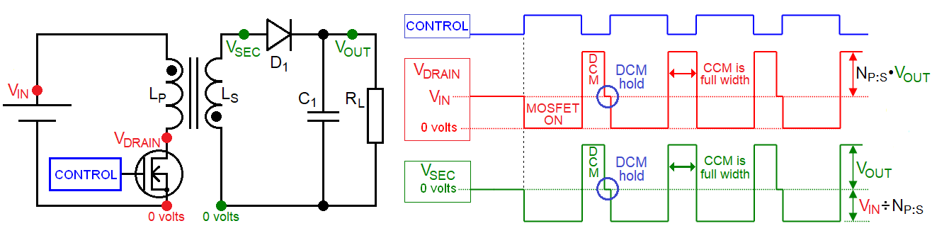
| When CONTROL is high the MOSFET activates (\(V_{DRAIN}\) = zero) |
|
|
\(\hspace{1.0cm}\) (1) (2) (3) (4) (5) |
\(V_{IN}\) is applied across the primary inductance \(L_P\) The primary current \(I_P\) rises linearly as it would in any inductor The core's magnetic flux also rises with the rising \(I_P\) \(V_{SEC}\) is negative due to the transformer dot arrangement \(D_1\) is reverse biased and zero secondary current (\(I_S\)) flows |
When CONTROL is low the MOSFET deactivates (flyback occurs) |
|
|
\(\hspace{1.0cm}\) (1) (2) (3) (4) (5) (6) (7) |
Secondary voltage \(V_{SEC}\) is now positive and forward biases \(D_1\) Energy begins to transfer to \(C_1\) and \(R_L\) \(I_S\) (and core magnetic flux) fall at a rate that sustains \(V_{OUT}\) This back-induces a voltage at \(V_{DRAIN}\) via transformer action Some time later, the core flux and \(I_S\) may fall to zero (DCM) and... The back-induction to \(V_{DRAIN}\) ceases (HOLD period) or... \(I_S\) doesn't fall to zero (CCM) and the charging cycle restarts |
It may be easier to consider the single inductor equivalent circuit when analysing DCM and CCM current waveforms: -

- S1 replaces the MOSFET
- L1 replaces the transformer
- S2 replaces diode D1
- DCM (discontinuous conduction mode) - inductor current will fall to zero amps. Accommodates light to medium load currents. Duty cycle lower than CCM. S1 and S2 will both turn off when the inductor energy is depleted.
- CCM (continuous conduction mode) - inductor current remains above zero amps. Accommodates medium to heavier load currents. Duty cycle higher than DCM. S1 and S2 are never both off. There is always residual magnetic energy.
DCM has three distinct phases per switching cycle; charge (red), transfer (green) and hold. The length of the hold-phase accommodates load current variations: -
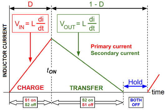
Load current variations are accomodated by changing the duty cycle (lengthening or reducing the hold period): -
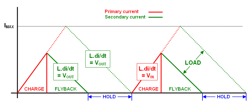 If the load requires more power, then the hold period shortens whilst maintaining current rise and fall slopes. The "hold" period
has a variable length; if the load is light, the energy transferred during flyback has to match the energy requirements of the load
in order to keep \(V_{OUT}\) at a constant value. This is important in the DCM design - on very light loads, the charging and flyback
times need to be small and, the hold period becomes long. Not so in CCM.
If the load requires more power, then the hold period shortens whilst maintaining current rise and fall slopes. The "hold" period
has a variable length; if the load is light, the energy transferred during flyback has to match the energy requirements of the load
in order to keep \(V_{OUT}\) at a constant value. This is important in the DCM design - on very light loads, the charging and flyback
times need to be small and, the hold period becomes long. Not so in CCM.CCM has just two phases; charge (red) and transfer (green). Load current changes are accommodated by the whole of the inductor current waveform rising or falling: -
\(V_{OUT}\) is no longer dependent on the load current because the average inductor current rises or falls to suit the load.
Accommodating the full \(V_{IN}\) range (DCM example)
When \(V_{IN}\) has a range of values, notice that the green-line slopes are fixed indicating that \(V_{OUT}\) is maintained: -
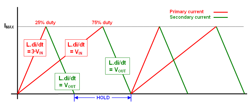
The above is an example when the \(V_{IN}\) range varies by 3:1. This range might attract duty cycles from 25% to 75%.
DCM and CCM summary
Only one mode will deliver the required output voltage to the load
- Lighter loads are usually serviced in DCM
- Heavier loads are usually serviced in CCM
- CCM is a natural outcome when DCM can't service the heavier load
- DCM is a natural outcome when CCM can't service the lighter load
- In DCM, the output voltage IS load dependent
- In CCM, the output voltage is NOT load dependent
DCM / CCM Boundary
This is where DCM meets CCM; the inductor has delivered all it's energy to the output and the switching cycle restarts immediately. We then need to ask this hypothetical question: -
$$\color{red}{\boxed{\text{Is the boundary power transfer more than that required by the load}}}$$
- If the answer is yes, then we will operate in DCM.
- If the answer is no, we will operate in CCM.
To calculate the boundary power transfer we need to establish the boundary duty cycle (D). From D we can calculate the peak primary current. And, from the peak current we can calculate the magnetic energy stored. From the stored energy (knowing the switching frequency) we can calculate the boundary power transfer.
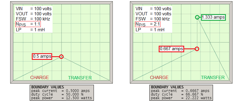
The boundary duty cycle (D) is trigonometrically constrained by \(V_{IN}\), \(V_{OUT}\) and the turns ratio \(N_{P/S}\): - $$D = \dfrac{N_{\text{P:S}}\cdot V_{OUT}}{N_{\text{P:S}}\cdot V_{OUT}+V_{IN}}$$ Here are examples of a 1:1 transformer (left) and a 2:1 transformer (right). Boundary limits are shown: -
So, once we have calculated D at the boundary, we can find \(I_P\) using the basic inductance formula: -
$$V_{IN} = L_P\cdot \dfrac{di}{dt}$$ But we need to find \(dt\) first: -
$$dt = D_{BOUND}\cdot \text{switching period} = \dfrac{D_{BOUND}}{F_{SW}}$$ Once we know \(dt\) the primary peak current is: - $$I_{P} = di = dt\cdot\dfrac{V_{IN}}{L_P}$$ Knowing \(I_P\) we can calculate the peak energy using: - $$\text{Energy} \hspace{1cm}=\hspace{1cm} \dfrac{1}{2}\cdot L_P\cdot I_P^2 \hspace{1cm}=\hspace{1cm} \dfrac{1}{2}\cdot L_P\cdot \left(dt\cdot\dfrac{V_{IN}}{L_P}\right)^2$$ $$=\hspace{1cm} \dfrac{1}{2}\cdot L_P\cdot \left(\dfrac{D_{BOUND}}{F_{SW}}\cdot\dfrac{V_{IN}}{L_P}\right)^2\hspace{0.7cm} $$ The boundary power output is simply energy multiplied by the switching frequency. To cut a long story short: - $$P_{\text{BOUNDARY}} = \dfrac{V_{IN}^2\cdot D_{BOUND}^2}{2\cdot L_P\cdot F_{SW}}$$
Minimum loading is required
A flyback converter stores energy and releases it each switching cycle. Given that this is done many times per second, it should be regarded as a power regulator. It isn't a voltage regulator until you apply a control loop around the switching circuit to keep the output voltage regulated by modifying duty cycle. This is why it is important to consider the light load scenario and the minimum duty cycle of the switching device. For instance, if the minimum duty cycle is 5%, there will always be some small amount of energy presented to the output each cycle AND, to prevent the output voltage rising continually, there must be a minimal load arrangement that consumes this small amount of energy per cycle.
DCM \(V_{IN}\) to \(V_{OUT}\) transfer ratio
Using \(V = L\cdot \dfrac{di}{dt}\hspace{1cm}\) and recognizing that \(\hspace{1cm}dt= \dfrac{D}{F_{SW}}\hspace{1cm}\)we can say: -
\(I_{PK}=\dfrac{V_{IN}\cdot D}{L_P\cdot F_{sw}}\tag{1}\)
The energy stored in inductor \(L_P\) is: -
\(\frac{1}{2}\cdot L_P\cdot I_{PK}^2\tag{2}\)
Substitute \(I_{PK}\) from (1) into the inductor energy formula we get: -
\(\text{Energy}=\dfrac{V_{IN}^2\cdot D^2}{2\cdot L_P\cdot F_{sw}^2}\)
Multiply energy by \(F_{SW}\) to get power: -
\(P=\dfrac{V_{IN}^2\cdot D^2}{2\cdot L_P\cdot F_{sw}}\)
Hence, \(\dfrac{V_{OUT}^2}{R_L}=\dfrac{V_{IN}^2\cdot D^2}{2\cdot L_P\cdot F_{sw}}\)
And therefore, \(\dfrac{V_{OUT}}{V_{IN}}=D\cdot\sqrt{\dfrac{R_L}{2\cdot L_P\cdot F_{sw}}}\)
The eagle-eyed will notice that the DCM output voltage is unaffected by the turns ratio \(N_{\text{P:S}}\). This is because in DCM we are transferring power i.e. the circuit is a power regulator. In CCM, the circuit behaves like a voltage regulator and, the transfer formula includes \(N_{\text{P:S}}\).
Flyback voltage considerations
In the default calculator example at the top of the page, a 1:1 transformer produces a \(V_{OUT}\) of 500 volts DC. During "flyback" (the transfer of energy), 500 volts also gets 1:1 reflected to the primary winding and this means that when the MOSFET DRAIN terminal will see the input voltage (125 volts) plus the 500 volts of flyback. This means that the MOSFET will need to be rated sparingly in excess of 625 volts to avoid damage.
To reduce this we can use a step-up secondary winding. For example, if a 1:2 step-up transformer is used then the secondary "flyback" of 500 volts is only 250 volts on the primary and, this means the MOSFET need not be rated much greater than 375 volts on the DRAIN. If a 1:4 transformer is used, the primary "flyback" is 125 volts and a MOSFET with a rating greater than 250 volts can be chosen.
Leakage Inductance considerations
There will always be energy stored in the primary that cannot be transferred to the secondary because the two coils will never be 100% coupled. The outcome of this is that when the MOSFET turns off, in addition to the fly-back voltage raising the drain higher than \(V_{IN}\) there will be an extra spike due to leakage inductance. This can be dealt with using a diode-capacitor-resistor snubber or a zener clamp: -
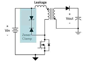
Note that the zener diode has to allow the normal flyback voltage to occur unimpeded hence, its voltage rating has to be greater than the natural flyback voltage seen on the primary winding during energy transfer.
Ω σ μ τ ω β δ η θ λ π ζ ∞ ° √ Δ ∂ ∫ Ʃ ± ≈ ≠ µ Ω ± ÷ Θ « » ≦ ≧ Σ Φ ε • θ λ ρ ω κ ² ³ ½ ¼ ¾ ° ∞ ∫≈ ≠ ≡ Ξ ∑ π Π © ®